
HDLBits(9)——Latches and Flip-Flops
----- 81. D flip-flop -----
Problem Statement
A D flip-flop is a circuit that stores a bit and is updated periodically, at the (usually) positive edge of a clock signal.
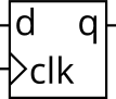
D flip-flops are created by the logic synthesizer when a clocked always block is used. A D flip-flop is the simplest form of “blob of combinational logic followed by a flip-flop” where the combinational logic portion is just a wire.
Create a single D flip-flop.
Answer
1 | module top_module ( |
----- 82. D flip-flops -----
Problem Statement
Create 8 D flip-flops. All DFFs should be triggered by the positive edge of clk.
Answer1
1 | module top_module ( |
Answer2
1 | module top_module( |
----- 83. DFF with reset -----
Problem Statement
Create 8 D flip-flops with active high synchronous reset(同步复位,高电平有效). All DFFs should be triggered by the positive edge of clk.
Answer
1 | module top_module ( |
----- 84. DFF with reset value -----
Problem Statement
Create 8 D flip-flops with active high synchronous reset. The flip-flops must be reset to 0x34 rather than zero. All DFFs should be triggered by the negative edge of clk.
Answer
1 | module top_module ( |
----- 85. DFF with asynchronous reset -----
Problem Statement
Create 8 D flip-flops with active high asynchronous reset(异步复位,高电平有效). All DFFs should be triggered by the positive edge of clk.
Answer
1 | module top_module ( |
==(批注:异步复位需要将复位信号写入敏感列表中,并且注明是上升沿(高电平)有效还是下降沿(低电平)有效;同步复位不用写入列表中)==
----- 86. DFF with byte enable -----
Problem Statement
Create 16 D flip-flops. It’s sometimes useful to only modify parts of a group of flip-flops. The byte-enable inputs control whether each byte of the 16 registers should be written to on that cycle. byteena[1] controls the upper byte d[15:8], while byteena[0] controls the lower byte d[7:0].
resetn is a synchronous, active-low reset(同步复位,低电平有效).
All DFFs should be triggered by the positive edge of clk.
Answer
1 | module top_module ( |
----- 87. D Latch -----
Problem Statement
Implement the following circuit:
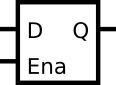
Note that this is a latch(锁存器), so a Quartus warning about having inferred a latch is expected.
Answer
1 | module top_module ( |
==(批注:若在always列表改成posedge ena,会综合出触发器(flip-flops))==
==(锁存器和触发器的区别是:锁存器对输入电平(使能信号)敏感,触发器对时钟信号敏感)==
----- 88. DFF (asynchronous reset) -----
Problem Statement
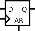
Implement the following circuit:
Answer
1 | module top_module ( |
----- 89. DFF (synchronous reset) -----
Problem Statement
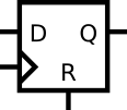
Implement the following circuit:
Answer
1 | module top_module ( |
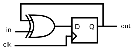
----- 90. DFF+gate -----
Problem Statement
Implement the following circuit:
Answer
1 | module top_module ( |
----- 91. Mux and DFF (a) -----
Problem Statement
Consider the sequential circuit below:
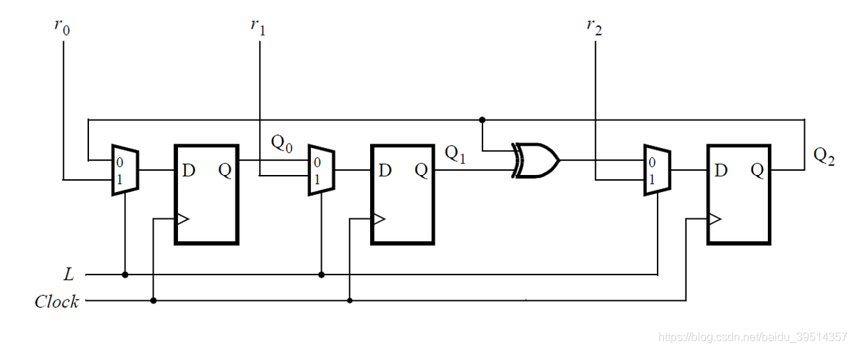
Assume that you want to implement hierarchical Verilog code for this circuit, using three instantiations of a submodule that has a flip-flop and multiplexer in it. Write a Verilog module (containing one flip-flop and multiplexer) named top_module for this submodule. ==(批注:写出子模块即可!!!)==
Answer
1 | module top_module ( |
----- 92. Mux and DFF (b) -----
Problem Statement
Consider the n-bit shift register circuit shown below:
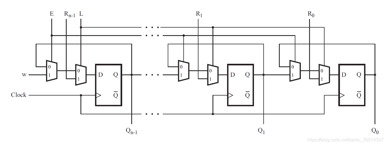
Write a Verilog module named top_module for one stage of this circuit, including both the flip-flop and multiplexers. ==(批注:与上题一样,写出子模块即可!!!)==
Answer
1 | module top_module ( |
----- 93. DFFs and gates -----
Problem Statement
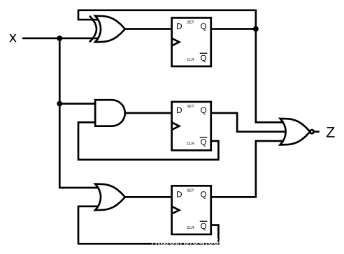
Given the finite state machine circuit as shown, assume that the D flip-flops are initially reset to zero before the machine begins.
Build this circuit.
Answer
1 | module top_module ( |
==(批注:若将qn = ~q写入always块中,将综合出两个D触发器,与题目要求不符)==
----- 94. Create circuits from truth table -----
Problem Statement
A JK flip-flop(JK触发器) has the below truth table. Implement a JK flip-flop with only a D-type flip-flop and gates. Note: Qold is the output of the D flip-flop before the positive clock edge.
| J | K | Q |
|---|---|---|
| 0 | 0 | Qold |
| 0 | 1 | 0 |
| 1 | 0 | 1 |
| 1 | 1 | ~Qold |
Answer
1 | module top_module ( |
----- 95. Detect an edge -----
Problem Statement
==(检测上升沿)==
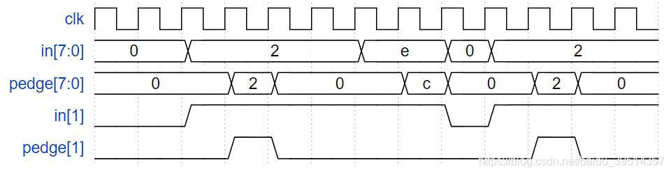
For each bit in an 8-bit vector, detect when the input signal changes from 0 in one clock cycle to 1 the next (similar to positive edge detection). The output bit should be set the cycle after a 0 to 1 transition occurs.
Here are some examples. For clarity, in[1] and pedge[1] are shown separately.
Answer
实现原理如下:

1 | module top_module ( |
----- 96. Detect both edges -----
Problem Statement
==(检测上升沿和下降沿)==
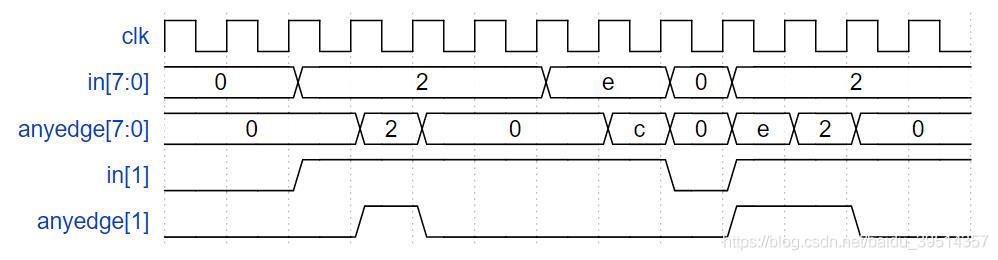
For each bit in an 8-bit vector, detect when the input signal changes from one clock cycle to the next (detect any edge). The output bit should be set the cycle after a 0 to 1 transition occurs.
Here are some examples. For clarity, in[1] and anyedge[1] are shown separately.
Answer
实现原理如下:

1 | module top_module ( |
----- 97. Edge capture register -----
Problem Statement
==(捕获输入信号的下降沿,捕获后维持高电平,复位后变为低电平,即为捕获寄存器)==
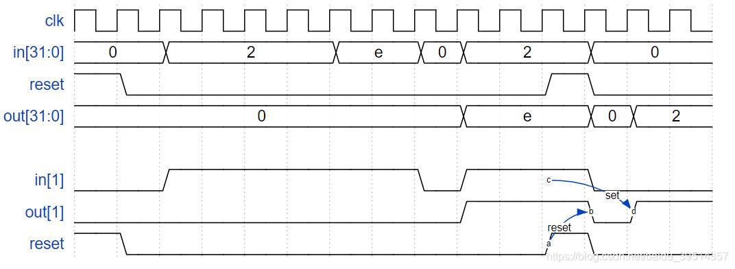
For each bit in a 32-bit vector, capture when the input signal changes from 1 in one clock cycle to 0 the next. “Capture” means that the output will remain 1 until the register is reset (synchronous reset)(同步复位).
Each output bit behaves like a SR flip-flop(RS触发器): The output bit should be set (to 1) the cycle after a 1 to 0 transition occurs. The output bit should be reset (to 0) at the positive clock edge when reset is high. If both of the above events occur at the same time, reset has precedence(优先权). In the last 4 cycles of the example waveform below, the ‘reset’ event occurs one cycle earlier than the ‘set’ event, so there is no conflict here.
In the example waveform below, reset, in[1] and out[1] are shown again separately for clarity.
Answer
实现原理如下:

1 | module top_module ( |
----- 98. Dual-edge triggered flip-flop -----
Problem Statement
==(双边沿D触发器)==
You’re familiar with flip-flops that are triggered on the positive edge of the clock, or negative edge of the clock. A dual-edge triggered flip-flop is triggered on both edges of the clock. However, FPGAs don’t have dual-edge triggered flip-flops, and always @(posedge clk or negedge clk) is not accepted as a legal sensitivity list(敏感列表).
Build a circuit that functionally behaves like a dual-edge triggered flip-flop:
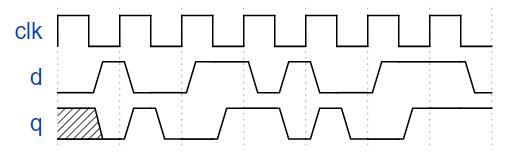
(Note: It’s not necessarily perfectly equivalent: The output of flip-flops have no glitches(脉冲,毛刺), but a larger combinational circuit that emulates this behaviour might. But we’ll ignore this detail here.)
Answer1
==(上升沿和下降沿触发要分开写)==
实现原理如下:

1 | module top_module ( |
Answer2
==(网站给出的解法比较巧妙,利用了异或运算的可交换性)==
1 | module top_module( |